O. Bierwagen (PDI), J. Schwarzkopf (IKZ), M. Bickermann (IKZ), K. Char (Seoul National University), M. Albrecht (IKZ)
Cluster G; Funded by the Leibniz association under Grant No. K74/2017
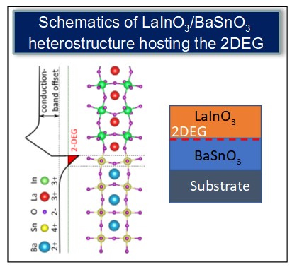
Realizing two-dimensional electron gases (2DEG) with high room-temperature (electron) mobility using perovskite oxides is the holy grail for multifunctional electronic devices. The interface between the lattice-matched perovskites LaInO3 and BaSnO3 is ideally suited for this purpose.
A team of bulk crystal growers, epitaxy, and electron microscopy experts from GraFOx cluster G laid the foundation to realize this interface with highest structural quality.

They developed the growth of bulk BaSnO3 [1] and LaInO3 [2] substrates for dislocation-free epitaxial growth of the heterostructure, demonstrated epitaxy of the individual layers [3, 4], and realized the heterostructure by pulsed laser deposition [5] and molecular beam epitaxy [Figures].
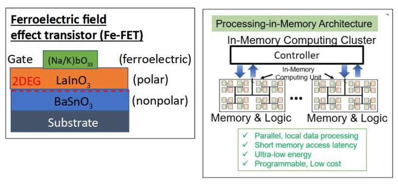
The 2DEG is induced by the combination of the polar and non-polar perovskites LaInO3 and BaSnO3. Epitaxial combination with further perovskites (chemical formula ABO3) allows to harness their physical properties (governed by the choice of cations A and B) to enhance the functionality of the 2DEG.
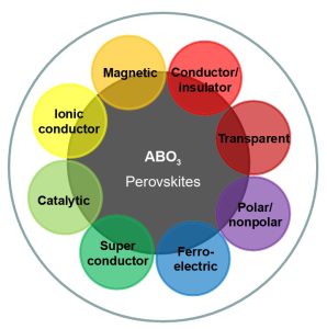
While the 2DEG itself can be applied in transparent field effect transistors (FETs), combination with a ferroelectric is projected to allow realization of a ferroelectric FET as a building block for energy-efficient in-memory computing or non-volatile memory.
[1]

