Kornelius Tetzner, Ferdinand-Braun-Institut
Cluster D, 16ES1084K
The semiconductor β-Ga2O3, characterized by its ultra-wide bandgap of around 4.8 eV, has gained significant interest in recent years with respect to the next generation of power electronic devices. The estimated high breakdown strength of 8 MV/cm and the resulting high Baliga’s figure of merit of >3,000 indicate that much more compact and therefore efficient power converters can be realized with this material compared to more established SiC or GaN technologies. In order to use the full potential of the material properties of β-Ga2O3 for high-voltage/high-current applications, a vertical device structure is preferred over a lateral design for active devices.
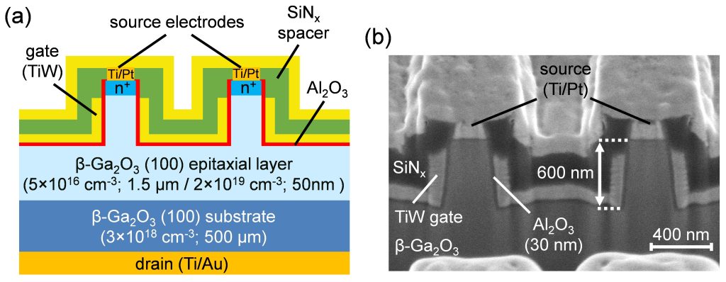
In collaboration with the Leibniz-Institut für Kristallzüchtung (IKZ), FBH has recently started activities to realize vertical β-Ga2O3 FinFET devices. The fabrication of such devices was carried out on epitaxial (100) β-Ga2O3 wafers realized at IKZ. Fin structures were formed using e-beam lithography and dry etch processing. Gate stack and SiNx spacer were patterned by photoresist planarization and self-aligned etching procedures.
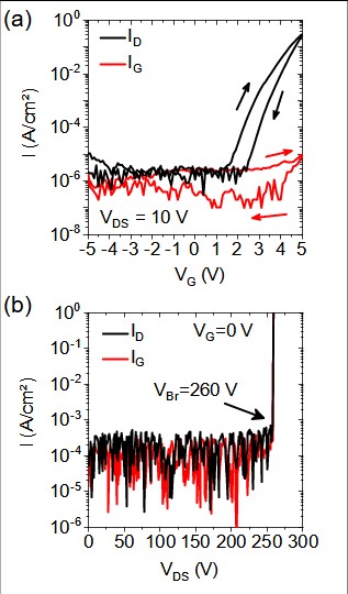
A representative transfer characteristic is presented in Fig. 2(a). It demonstrates decent device functionality with proper modulation of the drain current, featuring an on/off current ratio of around 105. Furthermore, the threshold voltage is around +4.2 V, thus emphasizing a normally-off characteristic of the device. In addition, three-terminal off-state breakdown measurements reveal an abrupt and catastrophic breakdown of the device at 260 V as shown in Fig. 2(b). This value corresponds to an average breakdown strength of around 2.7 MV/cm which is already much higher than what was previously demonstrated for vertical SiC- or GaN-based power transistors.
Thus, our investigations demonstrate the high potential of vertical FinFET architectures based on β-Ga2O3 to realize high-voltage transistor devices with improved efficiencies for next-generation power applications. It is expected that further development of such devices will significantly reduce power losses which can lead to energy savings in a variety of electronic applications.
Publication
K. Tetzner et al., Enhancement-mode vertical (100) β-Ga2O3 FinFETs with an average breakdown strength of 2.7 MV/cm, Jpn. J. Appl. Phys. 62, SF1010 (2023).