Cluster D
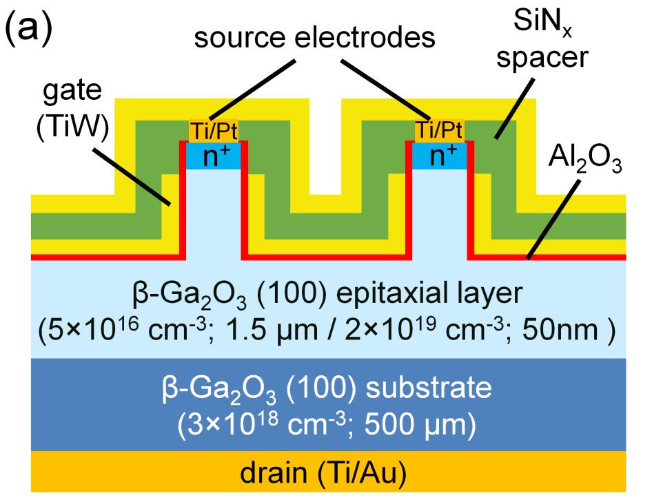
In collaboration with the Leibniz-Institut für Kristallzüchtung (IKZ), FBH has recently started activities to realize vertical β-Ga2O3 FinFET devices.
Vertical β-Ga2O3 FinFET devices
Cluster P
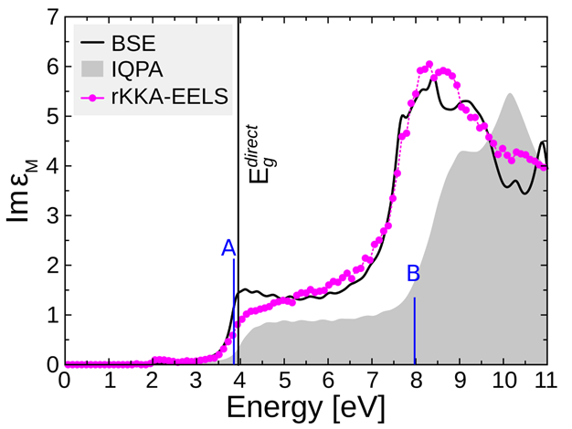
With the example of BaSnO3, this work demonstrates a fruitful synergy between different high-level theoretical and experimental methods for a quantitative comparison of excited-state properties of complex materials.
Excitations in cubic BaSnO3:a consistent picture revealed by combining theory and experiment
Cluster G
A team of bulk crystal growers, epitaxy, and electron microscopy experts from GraFOx cluster G laid the foundation to realize two-dimensional electron gases with high room-temperature mobility using perovskite oxides.
Realizing perovskite interfaces for high-mobility two-dimensional electron gases
Archive
Structural defects and charge carrier mobility in homoepitaxial layers grown on (100) plane of β-Ga2O3
Suboxide-related kinetics, etching, thermodynamics, and catalysis governing the MBE of Ga2O3, In2O3, SnO2 and (In,Ga)2O3
Ga2O3-based devices
Faceting and step flow growth in the homoepitaxy of Ga2O3
Barium stannate based heterostructures for electronic applications
β-Ga2O3 fundamental properties and their anisotropy
Joint computational and experimental examination of the phase stability of (In xGa1–x)2O3 ternary alloys
Anisotropy of optical and electrical properties of rutile SnO2
Finding the right balance for SnO growth enables the realization of all-oxide SnO/Ga2O3 vertical pnheterojunction diodes